

A professional or experienced PCB designer can easily tell which PCB design was done by an expert and which one was done by an amateur. Engineering students often fail to follow standards and practices in their PCB designs. These practices and standards are what separate them from professionals.
Electronics manufacturing companies, like MJS Designs, have perfected the art of PCB designing over the years. At present, they’re one of the leading PCB design and manufacturing companies in the US. MJS Designs has achieved this feat by ensuring industry standards in its designs and final products. Everything from their CAD designs to PCB assembly follows a strict and well-monitored process to ensure high standards and quality.
As an engineering student, you can’t put in the same effort as an electronics company like MJS Designs. However, you can do your best to maintain the standards and principles in the PCB design phase and make it look as professional as possible.
So, to help you out, let’s discuss the nine things you must ensure in your PCB design to make it look professional.
#1 Deciding on the Grid Space
Use a grid spacing that will fit all your components. Ideally, you want something that will allow maximum board usage. Remember that many components or devices come in various package sizes. So, you can always browse through those sizes in case the default or generic version doesn’t work for your grid.
Avoid using multiple grids as much as you can. Doing so will increase the complexity of your project. Using a standardized grid will reduce polygon-fill discrepancies, making your life much easier.
#2 Trace Lengths Must Be As Short As Possible
The shorter the traces (wires/connections) between components, the less complex the circuit. The best way to make traces shorter is by ensuring direct connections without any bends.
Another rule of thumb in this regard is to keep the core component at the center of the board. That will ensure that the core component is equidistant from all the other components, and the interconnecting traces between them will be short.
Longer traces can lead to impedance or noise. That means the signals through these traces will be jittery, leading to a drop in efficiency and performance.
#3 Distribute Power Lines Wisely
Apply adequate copper to common connections so that the power flow is as effective as possible. You can achieve this by using pours on the power plane. Doing so will minimize impedance and voltage drop.
Running multiple supply and ground lines is also a good way to ensure efficiency. Avoid runovers as they can lead to cross-talk and hamper the signals through the traces.
#4 Know Which Components You Can Group
Grouping the components can help shorten trace lengths. You should consider grouping components that require the same amount of power, capacitance, or resistance.
Also, consider grouping the components having plenty of traces coming in and out of them. Placing them in the center of the board should make the PCB design look less messy and more professional.
#5 Panelize the PCB
Suppose you start with a particular board size but at some point realize that you need something bigger. In such situations, replicate the existing board and add it to the design. Doing so will give the PCB a panel-like design. Each panel you add will be the original board you started the design with.
Keep adding the panels until the desired size is reached. You can also reduce the panels if you need to make the design smaller. This building-block model helps manufacturers design PCBs that might need additions in the future.
#6 Keep a Bit of Space Near the Edges
To make your design more practical, it’s a good idea to leave some space near the boundary or edge of your PCB design. Manufacturers can utilize that space to fit screws or mounting holes. So, when you have to mount the PCB on a device, you can do so using screws and don’t have to weld anything.
Designers often forget to leave this space. However, an experienced PCB design company will notice it. Companies like MJS Designs know how PCBs work, which is why they take it upon themselves to leave a bit of space while printing the PCB.
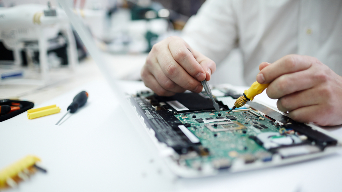
#7 Test and Debug
PCB printing companies will do the testing and debugging for you. However, it’s a good practice to do so yourself. Generate personalized data if necessary and run it on your PCB.
Apart from checking for logical errors, look for issues in the components. Use a multimeter to check whether or not the connections are working correctly and if all the components are getting the power they need.
#8 Leave Space between Traces and Mounting Holes
When placing the mounting or screw holes on your PCB, ensure they’re not touching the traces or getting too close to them. You need to leave some space between the holes and the traces. Otherwise, it can lead to shock hazards.
#9 Keep Heat-Sensitive Components Away from Heat Generating Components
Components like bridge rectifiers, diodes, MOSFETs, inductors, and resistors generate a lot of heat when they’re operational. The heat from these components can affect heat-sensitive components like thermocouples and electrolytic capacitors when they’re too close to one another. The heat will reduce the sensitive components’ longevity and lead to false or anomalous temperature readings.
For now, that’s all you need to know about PCB design principles. You’ll make a few mistakes along the way, but that’s part of the learning process. So, don’t worry about that, and stick to the basics. You’ll eventually get better at designing these boards and making them more efficient.


